


Header overlays
Labels → Header Overlay creates a single artwork item containing a legend for a row of pins. Stable 1.4.1 supports single-row 2.54 mm headers. Generalized standard/custom pitches belong to the development tools.
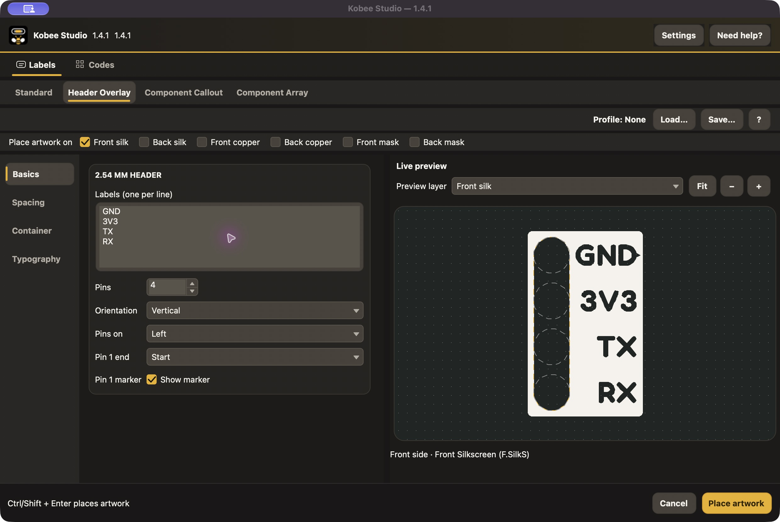
Make a four-pin serial connector legend
Section titled “Make a four-pin serial connector legend”-
Measure or inspect the connector footprint. Confirm that it is a single row with 2.54 mm pitch and identify physical pin 1.
-
Open Labels → Header Overlay.
-
Set the pin count to 4 and enter one line per pin:
GND3V3TXRX -
Choose Orientation, the side the Pins occupy, and the Pin 1 end. Compare the label order to the actual footprint; the first line is not automatically the pin nearest the screen’s top-left corner.
-
Enable the optional Pin 1 marker if you want an additional assembly cue.
-
Choose the enclosure style, text height and connector clearances.
-
Select the target layer, preview and place. Align the generated artwork to pin 1 in KiCad, then check the far end against the last pin.
The tool does not rename pins or change the electrical connector. Treat its text as a legend that must be checked against the schematic, pin numbers and real mating orientation.
Orientation and label order
Section titled “Orientation and label order”Horizontal and vertical layouts change the arrangement of the row. Pin-side and pin-1-end controls determine how the text sits around it. Change these before fine-tuning margins: rotating the finished footprint in KiCad is different from changing which side of the pin row contains the labels.
A useful check is to use the deliberately asymmetric sequence 1, 2, 3, 4 on a test item, place it next to the connector and verify every position. Then replace the numbers with signal names. This exposes reversed order more clearly than a repeated GND label.
Fit around the connector, not just the pads
Section titled “Fit around the connector, not just the pads”Reserve space for the physical plug or shroud. A legend that clears the copper pads can still be covered by an installed connector.
| Control concept | What it changes |
|---|---|
| Pin/plug envelope | The space reserved for connector hardware |
| Pin-to-label gap | Distance between the connector region and text region |
| Label-side padding | Space beyond the labels toward the outer edge |
| Leading/trailing padding | Enclosure extension before pin 1 and after the last pin |
| Opening width | Width removed for a continuous plug or individual pin openings |
| Opening end extension | Extra opening beyond the end positions |
| Text height | Physical size of each pin name; it must fit the available pitch |
Use the connector datasheet or a physical measurement for a shrouded plug. Extra enclosure padding does not necessarily create a larger opening; adjust the clearance/opening controls that correspond to the actual collision.
Choose an opening
Section titled “Choose an opening”The tool offers None, a continuous plug opening, and individual pin openings.
- Choose None for suitable silkscreen artwork when you do not need a geometric hole in the enclosure. KiCad/fabricator silk clipping still needs checking.
- Use a continuous opening for a single clear connector region, particularly for a plug body.
- Use individual openings when separate per-pin holes fit the intended design.
For copper output, the tool requires an opening to reduce the risk of joining pins with the generated fill. That guard does not replace electrical clearance checks: inspect every pad, net and opening in PCB Editor and the final Gerbers.
Enclosure and long edges
Section titled “Enclosure and long edges”Filled/inverted and outline appearances are available. Independent long edges controls the pair of corners along the pin side and the pair along the label side. It does not mean “pin-1 end versus far end.” Use the radius control to make rounding subtle enough for the actual enclosure dimensions.
Label padding, connector clearance and corner radius interact. Check a longer signal name before finalizing a compact rail: the count and longest label can change its overall dimensions.
Editing a connector later
Section titled “Editing a connector later”Select the generated artwork footprint and reopen Kobee Studio. If the connector gains a pin, update both the pin count and label lines. Review all labels and their order after the count change, then compare the first and last positions to the electrical footprint again.
The overlay and connector are separate footprints. Moving the electrical connector does not imply that the artwork will follow it automatically. Move the artwork with it and recheck alignment.
Final connector checklist
Section titled “Final connector checklist”Confirm pin 1, line order, pitch, actual plug-body clearance and optional marker. Check the bottom-side reading direction if applicable. Export the silkscreen Gerber with the same solder-mask clipping options you will use for production; a perfect editor overlay can still be clipped around mask openings. Follow the layers and fabrication checklist.